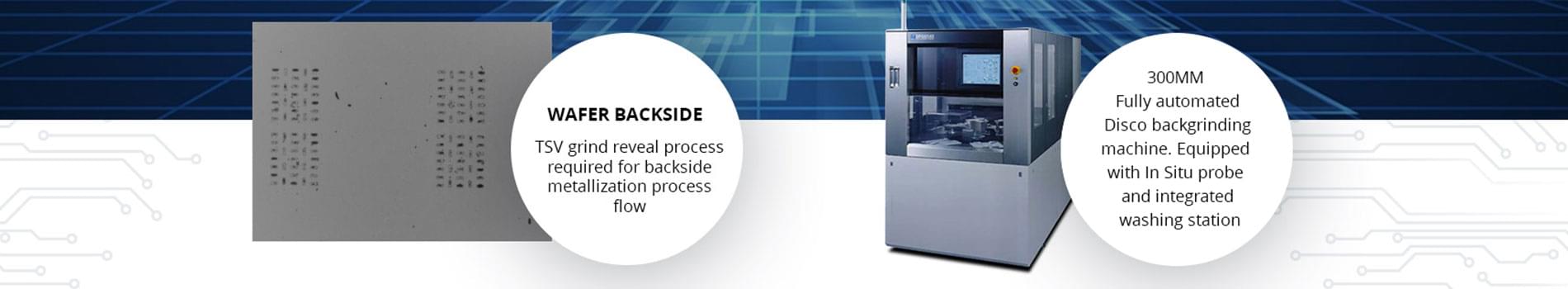
Backgrinding & Stress Relief
GDSI delivers complete backgrinding solutions to the semiconductor, MEMS and biomedical industries. Backgrinding is a necessary process step to reduce wafer thickness prior to dicing and final assembly. By utilizing fully automated grinders staffed by highly qualified engineers, GDSI’s grinding procedures produce unsurpassed precision and repeatability.
- Individual chip grinding
- Wafer rounds up to 12” or 300MM
- Ultrathin wafers (<100um final thickness target)
- Waxless process
- Use of UV and non-UV tapes
- Thermal release tape for fragile device layers and ESD sensitive devices
- Excellent flatness uniformity and removal accuracy
- Bumped wafer layouts
- Temporarily bonded wafers
- SOI wafers
- TSV reveal for advanced wafer level package concepts
- Able to control surface roughness profile and bow warp
- Poligrind wheel available
- (CMP/Stress Relief Polishing) Up to 8” or 200mm
- Mirror finish
- Clean: SC1 available
Si, SiGe, SiC, Al2O3, glass, GaN & piezoelectric materials
Disco DFG 8540, Disco 850, DAG 810, Gigamat polishers
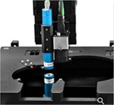
GDSI recommends FRT of America for your wafer measurement applications, performed
with non-contact technology.
Contact GDSI to learn more about FRT’s contract services or equipment sales

Core Capabilities using FRT technology
TOPOGRAPHY, PROFILE
- Roughness, waviness
- Step height
- Radius of curvature
- Thickness
WAFER INSPECTION
- TTV
- Bow
- Warpage
- flatness
Wafer thickness & flatness validation
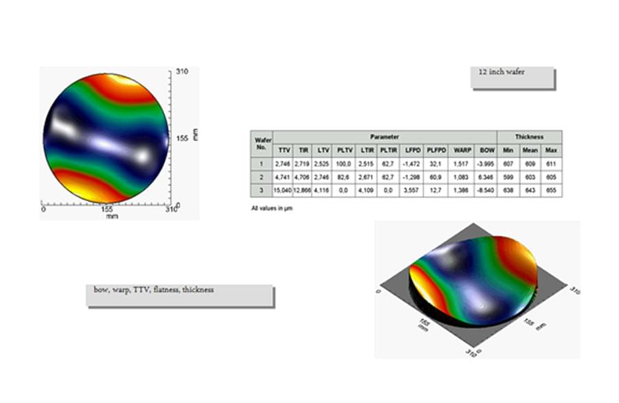
ttv Option
Both, the tabletop tool and the standalone systems of The Microprof series include the option for two-sided sample inspection which enables measurement of both sides simultaneously. The total thickness variation (TTV) of the sample can be determined along the surface parameters (e.g., roughness, waviness, and flatness) of both surfaces. The TTV option can be easily retrofitted at your site.”