Wafer Dicing
Dicing: Precision, Control & Repeatability
We have documented nearly 30 years of dicing experience. As a global supplier for complex dicing programs, GDSI anticipates future challenges by investing in advanced processes and tooling required to complete the assignment. Mechanical dicing is a well understood technique applied to a wide array of material types but may be ill suited for trends toward product miniaturization, MEMS and WLCSP. Smaller transistors enable increased density, low power consumption, lower cost per transistor and faster switching. At the same time, this trend poses vexing problems for wafer singulation due to the adoption of Cu/low-k dielectrics, shrinking scribe line widths, ultra-thin wafers and many other physical hurdles. GDSI and its valued OEM partners are well suited to address your individual requirement whether it calls for an optimized saw process, Stealth laser dicing process or any combination of mechanical and laser disciplines to get the job done.

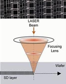
Complicated reticle field or multi product wafer. Diced with Stealth laser process by turning the laser on and off intermittently. Complete cleavage of all device types and cut using imported GDS file from customer

Cut intersection created by the Stealth laser
dicing process. No water and no particles
- Dry, water-free dicing using Stealth Laser Dicing Process
- Fully automated process flows with integrated cleaning (saw)
- Any size or shape up to 300MM or 12″
- Reticle subdicing
- Complex MPWs
- Advanced dicing methods for ultra-thin die (“Dice Before Grind”)
- Package dicing
- Thick wafer applications
- Low-k dicing strategies
- High Throughput & small NPI programs
- Wafer coring or downsizing
- Edge trimming and bevel cuts
- Multiple Disco dual spindle systems
- Stealth laser dicing system for MEMS and dry requirements
- ADT system for abnormally thick substrates & coring

